This section is prohibited for viewing by children.
Question 1:
That is, when a current flows in a conductor, does this mean that the electron moves with acceleration or not ???
I understand the process...
An electron, being in an atom, exchanges photons with the nucleus of an atom with a proton and immediately absorbs them.
When an electron breaks away from an atom and starts moving in a direction, it emits photons.
Why???
I went through the books and did not find a clear answer, but I came across mail.ru, where one physicist answered that each electron is dressed in a photon coat. And when the electron starts moving, this photon coat flies off the electron and, accordingly, twists like a whirlwind.
Have you heard of her so far? 
Essentially a misunderstanding of visual perception: adult beliefs in visual outliers, about 50% of today's adults believe in the outlier theory. What is the light that will splash on this orange in front of you and which is then reflected and received by your eyes? What you have is orange, it's spherical, and the texture resembles orange. But light can do so much more! He can tell you exactly which chemical composition objects you never see or touch, from stars like the Sun and the atmospheres of various planets to giant dust and gas clouds like the Orion Nebula.
Since the electron has a spin, the photons spin first in one direction when the electron moves in one direction, then in the other direction when the electron moves in the opposite direction.
That is, right: even when we are in the explorer D.C., then it is also considered that the electron moves with acceleration.
That is the electromagnetic field. So photons are emitted by electrons???
We can tell exactly which chemical elements are made just by looking at the light they emit or reflect. And we can only do this by Robert Bunsen and Gustav Kirschoff, the great bosses and pharaohs who invented one of the most important tools of the entire past and modern science: spectroscope. You cannot confuse them, neither is like the other. A spectroscope is simply an instrument with a glass prism in the middle that is designed to break the light received from a source into its component parts and project it onto a screen.
With radiation, what gives us an electric field, what function does it carry.
With magnetic it is clear, it cannot be if it does not electric field. Since the electric field just generates the directed movement of charged particles.
And for the receiving antenna, only photons are important?
Photons fly in a rotating pancake to the receiving antenna. In the receiving antenna, the orbitals of electrons line up for interaction, and begin to move in the opposite direction, emitting photons going towards the arriving ones.
Spectrum with absorption lines
Why do we do this and what helps us? 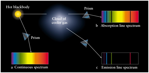
Look at the image above and say you have something like this: a light source, a glass prism and a screen. We have three ways in which we can use a prism. This is a continuous spectrum. If you put cold gas between a prism and a lamp, something strange happens: the light from the lamp passes through the gas, which absorbs some of the photons, leaving only a fraction of them. A rainbow will appear on the screen, but it will be interrupted by black lines representing the missing photons absorbed by the gas.
Times arise induction currents, so there is an opposing magnetic field.
Hence, the photons must also fly towards.
This is where the question arose about their interaction with each other.
Who thinks what is inside the electron?
I'm trying to shovel through the literature and make some sense of it all.
Here are the main chaotic thoughts:
1. An electron can be born in β-decay (this is a type of radioactive decay)
This is the signature of this gas. Depending on where and where the black lines appear, we can easily conclude which chemical element we are talking about. This is the spectrum of absorption lines. Now the spectrum looks completely different. Instead of having black lines on a rainbow background, we have some colored lines on a black background.
The difference is that the light does not come from the light that sends photons through the cold gas, but the gas itself heats up and emits light. This is the radiation spectrum. Now, whether or not you see the signature chemical element through the absorption spectrum or the emission spectrum, it's the same. Just in the first case, the element transmits the light emitted by the source, and in the second case, the chemical element itself is the source of light.
2. An electron is somewhat similar to the earth. (it also has magnetic poles)
By the way, I thought that the north pole is the north pole, the south pole is the south.
They just briefly talked about it at school, but didn’t attach any importance then.
The North Pole is the physical South Pole. That is, magnetic lines enter the top of the Earth
The South Pole is the physical North Pole. Magnetic lines coming out of the bottom of the earth
With this technique, we were able to find out, for example, what is the chemical composition of the atmosphere of Hyades, a star cluster 153 light years away. We didn't even have to travel there to find out that the stars in this swarm contain carbon, sodium, iron, nickel, and so on. If you look closely, you will see some absorption lines there. 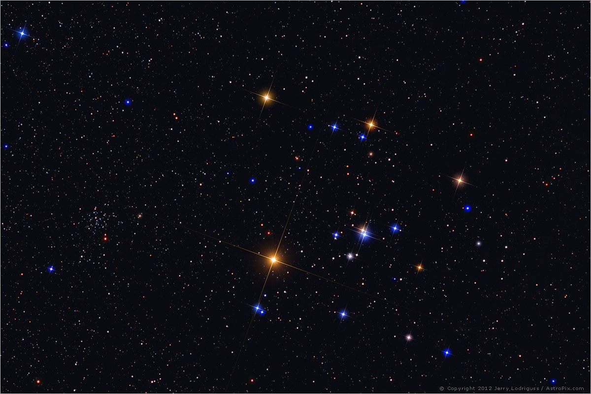
Also thanks to spectroscopy, we also discovered element #2, helium. The funny thing is that only 14 years old was discovered on Earth by physicist Luigi Palmeri. Until then, it was believed to exist only in space, so this chemical element was named Helios, the Greek name for the Sun.
The Earth also revolves around the core, and if you put a universal magnet next to the Earth (maybe a black one also has magnetic properties?), then the Earth should also, logically, emit photons. (Photon coat, that is)
And there is a reason why - the earth has a core that emits them.
3. An electron has some kind of energy, since it is dressed in a photon coat.
Oh, and something else, the element's unique signature not only occurs in the visible light spectrum, but you can find emission or absorption lines in both infrared and ultraviolet. But in this post we are talking about visible light, so we usually focus on it. And if you don't believe me, check out below the spectral signatures of each chemical element. As you can see, absolutely nothing happens.
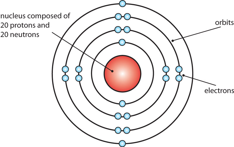
The funniest phase with these chemical signature signatures is that we've discovered and used them long before we know what it's producing. The revelation happened when Niels Bohr came with his new atomic model: an atom consisted of a nucleus, around which lay some electrons in circular orbits. Each such orbit can contain the maximum number of electrons, and electrons can only sit on these energy levels.
Conclusion: it means that the electron must have a very powerful nucleus in which undamped reactions occur in the form of generating these same photons.
Maybe nonsense, but maybe there is still a piece of a proton? It's just that the proton is in the nucleus - it turns out to be more positive, and then the electron is more negative.
Thanks in advance!
© Zvezdin A.K.
As expected, as in the case of absolutely everything and phenomena in this nice universe, the explanation concerns atomic or subatomic particles. You see that electrons on atoms can jump from one energy level to another energy level. That is if they get the energy they need. Haven't you understood a lot? This is a concept of quantum physics, rather abstract. 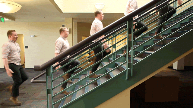
You want to jump a step: maybe the first step, the third step, or maybe the last step of the ladder. We know you can't land anywhere between stairs and you can only sit one step at a time.
- Now imagine that you are at the base of some steps.
- You are an electron and each step is an energy level of an atom.
Quantum mechanics of trapped photons
Optical microcavities, waveguides, photonic crystals
A.K. Zvezdin
Anatoly Konstantinovich Zvezdin, Doctor of Physical and Mathematical Sciences, Prof., Ch. scientific collaborator Theoretical Department of the Institute of General Physics named after A.M. Prokhorov RAS.
When talking about quantum mechanics, first of all, associations associated with the electron arise: “wave-particle” dualism, the Schrödinger equation, quantization of electron energy levels in atoms, etc. A photon (a quantum of an electromagnetic field) is, as it were, in the background. Of course, this elementary particle is very important from a conceptual point of view, but in quantum mechanics it is considered mainly as an intermediate agent in problems where the interaction of radiation and matter is studied.
What are you doing? You jump and jump and land on the first stage. However, how much you did, you needed a certain amount of energy. You return to the stairs and now jump on the third stage. You also needed a certain amount of energy to get there, but a little more than you needed to get to the first level. If you want to jump on the stairs, you need more energy than the first two days.

At any stage you want to jump, you need a certain amount of energy to get there. You can't jump to the head of a ladder with the same amount of energy you use to reach the first step, can you? This also happens with electrons: they need a certain amount of energy to reach a certain level of energy. The higher the energy level, the more energy is required. This thing is perfectly valid when it comes to the fact that not all electrons are on the first energy level.
The state of an electron can be arbitrary, both bound (for example, in an atom) and free, and is determined by external fields acting on the electron. It, more precisely, the wave function of an electron, is calculated using the Schrödinger equation, which makes it possible to find the energy spectrum of an electron (the dependence of its energy on momentum).
Some of them are higher and when they are mixed they come down. The one thing that's especially important about electrons is that if they don't get the right energy to go into an energy level, they just stay there. When the hydrogen gas receives heat, light or electricity, the electrons of the hydrogen atoms get into photons with energy. If a photon hits a hydrogen electron and has the correct energy, the electron jumps to a different energy level.
But here's the trick! After the jump, the electron reaches more than high level energy, but becomes agitated and wants to return to his original place. Definitely. And he captures it when he emits a photon that has the same energy as the one he received and that matches the color.
Unlike an electron, a photon is usually considered a free particle with energy E = ћ w and momentum p = ћk, where w- frequency, k - wave vector (|k| = k = 2 p/l, where l- wavelength), ћ - Planck's constant. The energy spectrum of a free photon is continuous (as for a free electron) and is characterized by the well-known electromagnetic wave dispersion law
In the ether, which we talked about in the last chapter, we are talking about the energy released by the electrons when it returns to its place. The absorption lines represent the energy received by the electrons in order to be able to jump to a certain energy level.
So practically, the electron gets energized, moves, realizes that it doesn't like where it was going, gets angry and says, “You know something? return your energy and leave me alone”, return the received energy and return it to its original place. Given that each chemical element has a certain number of electrons in a certain way, it is normal for them to proceed differently from one energy level to the next in terms of the energy received. Hence the unique signature of each chemical element.
c = w k. (one)
If the photon is in a transparent substance with a refractive index n, then instead of the speed of light c in formula (1) one should substitute u = c/n. The difference in the behavior and description of the electron and photon is explained by the fact that the electron has electric charge, so it is easy to influence its state electromagnetic interaction. A photon in such a picture is presented as something that cannot be controlled and controlled by external influences.
How to localize a photon?
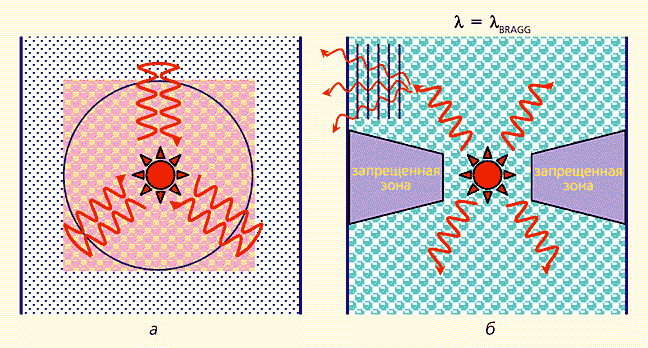
However, at the end of the XX century. the situation with photons has changed. New optical materials, structures, and devices have been created in which the motion of photons is far from being free, but rather resembles the motion of electrons in atoms, molecules, and crystals. The simplest such structure is an optical microresonator; a cavity whose walls have a high reflection coefficient in a certain frequency range. Obviously, the motion of a photon is limited by the internal volume of the cavity. In the English literature, this property of a quantum particle is denoted by the word “confinement”, i.e. “confinement in a closed space”, or more briefly - “captivity”. Therefore, it is natural to call a photon enclosed in a microresonator captive, or localized*. As with a bound electron, the energy spectrum of a trapped photon becomes discrete.
* The problem of photons localized in space has long occupied the classics. It is said that the last drawing by Bohr on a blackboard in his office at the Carlsberg Palace on the evening before his death (which followed on November 18, 1962) was a drawing of an Einstein photon box, which was directly related to one of the main issues in Bohr's discussions with Einstein.Properties close to those of a microresonator are, for example, a film or thread consisting of a transparent material with a higher refractive index and surrounded by a medium with a lower refractive index. Fiber optics is based on this principle. Again, by analogy with an electron, we can say that a medium with a higher refractive index acts on a photon, like a potential well on an electron, i.e. keeps it in the appropriate area of space.
A more complicated situation is realized in new artificial optical materials - photonic crystals. This term was introduced into scientific use in 1987 by E. Yablonovich, emphasizing that the energy spectrum of a photon moving in a photonic crystal is similar to the spectrum of an electron in a real crystal, for example, in a semiconductor. Almost simultaneously, similar results were published in the work of S. John.
Fig.1. The dependence of the refractive index on the coordinate (a) and a schematic representation of the structure of photonic crystals (b):
one-dimensional (1D), two-dimensional (2D) and three-dimensional (3D).
A photonic crystal is a spatially inhomogeneous structure characterized by a periodic function n(x, y, z), where n is the refractive index of the material (Fig. 1a). On the whole, the picture resembles the potential relief for an electron in a crystal. A band gap is also formed here - a certain frequency range in which the free propagation of a photon is prohibited. The photonic crystal-semiconductor analogy turned out to be very fruitful for the design and creation of new optical materials and devices, which significantly expanded the possibilities of optoelectronics and information technologies. In fairness, it should be noted that as early as 1972, the Russian physicist V. Bykov from the Institute of General Physics published a number of important results related to such periodic media. Apparently, his work and the work of other authors on this topic were done too early, when the situation was not yet ripe and the attention of researchers was focused on other directions that were more relevant at that time. In addition, the catchy term “photonic crystal” played a significant role in the boom initiated by the works [ , ]. Another famous French mathematician A. Poincaré noted that it is enough to invent a new word and this word becomes a creator.
Stimulated interest and practical needs: light is attractive because it can carry very large flows of information. Thus, the frequency band of a fiber-optic cable (~10 12 Hz) is many orders of magnitude higher than the frequency band of an electrical conductor of the same diameter. Another intriguing prospect is to control the intensity of spontaneous and induced emission of atoms and molecules located in photonic crystals or optical microcavities in order to increase the efficiency of various light sources: from incandescent bulbs to lasers.
Make it shine, not warm
It is well known that when an electron passes between energy levels E n and Em m, a photon is absorbed or emitted. The probability of such a process, for example, the process of spontaneous emission of a photon, is proportional to the density of photon states g( w) at a frequency w= = (E n – E m )/ ћ. Roughly speaking, g( w) is the number of photons having frequencies ranging from w before w + Dw, which can be “placed” in a volume unit (1 cm 3 ). For free photons, the density g(w) depends only on the frequency and is (Fig. 2.)
g( w) = w 2
/ (p 2 c 3 ). (2)
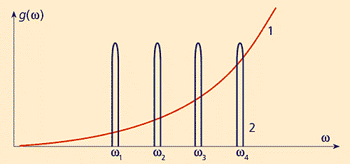
Fig.2. Densities of states of a free photon (1) and a photon localized in a 3D microresonator (2).
It determines, in particular, the radiation intensity of a body heated to a temperature T (for example, incandescent bulbs): intensity I( w) is the product of the photon energy ћ w, the number of possible places for it g( w) and the corresponding probability of filling these places. Considering that the latter is given by the Planck function, we obtain a very low intensity of visible light sources based on thermal radiation (incandescent lamps, etc.). Figure 3 shows that even when using the most heat-resistant tungsten filaments (T ~ 2000°C), the main part thermal radiation falls in the infrared range and only a small part (~5%) falls into the visible range. Incandescent lamps mainly heat the surrounding space, and do not shine. Using optical microresonators and photonic crystals, it is possible to increase the light output and the efficiency of heat sources. What is the essence of the idea?
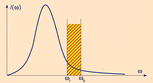
Rice. 3. Radiation intensity spectrum I( w).
The shaded area shows part of the total distribution,
within the visible range.
If we could redistribute the density of photon states g( w) so that it is maximum in the visible region of the spectrum and much smaller (ideally, it would turn to 0) in the IR range, then the light output, i.e. the ratio of the light energy of the radiation to the total energy would increase substantially. Controlling the geometric and physical parameters of photonic crystals and microresonators makes it possible to do this.
In the simplest flat optical microcavities, photon propagation along the z axis is limited by metal mirrors (Fig. 4a) or so-called Bragg mirrors (Fig. 4b). The latter are systems of alternating thin dielectric layers designed in such a way that, due to the interference of successively incident and reflected rays, the passage of light through the mirrors is completely extinguished. As the main and auxiliary layers, for example, Ga 1-x Al x As semiconductors with different x values are used; the technology of applying and coordinating them with each other has recently been well developed. There are 1D microcavities - films in which there is one forbidden direction for the propagation of a photon, 2D microcavities - optical fibers in which free propagation of photons in two directions is prohibited, and 3D microcavities in which the photon is completely trapped (Fig. 1b ). In the latter case, the photon energy levels become discrete.
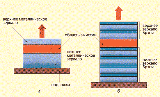
Rice. four. Planar microresonators:
with mirror walls (a); with Bragg mirrors (b).
Let the 3D microresonator have the shape of a parallelepiped with completely reflective walls, then the photon eigenfrequencies in it will be
w 2p,s,k = p 2 c 2 /n 2 (p 2 /a 2 +s 2 /b 2 + k 2 /c 2 ), (3)
where p, s, k are integers. The photon energy levels in the microresonator are defined as E 2 p,s,k = = ћ w 2p,s,k . The photon density of states here is a set of narrow peaks centered at points w 2 p,s,k (Fig. 2). By choosing the values a, b, c, n (as well as p, s, k), we can make the density g( w) is large (or, conversely, almost equal to zero) in the desired region of the spectrum. This fact was first published in 1947 by the American physicist E. Purcell and is called the Purcell effect. For a long time, such a possibility of controlling the photon spectrum and the probability of spontaneous transitions remained a theoretical prediction. AT last years the Purcell effect has been reliably experimentally confirmed.
We must make a reservation: the total reflection of light does not mean that all radiation is reflected on the walls. Indeed, a photon or a beam of light incident from an optically dense medium with a refractive index n 1 to the boundary with an optically less dense medium with a refractive index n 2 (n 2< n 1 ) под углом, бabout greater than the Brewster angle q B \u003d arcsin n 2 / n 1, experiences total internal reflection. However, an analysis of the Maxwell equations shows that in this case, instead of a transmitted wave in an optically less dense medium, a so-called lateral or side wave propagates along the surface, the amplitude of which decays as exp(– a z), where z is the normal distance from the boundary, a- attenuation parameter. And if another optically dense medium with n = n 1 is placed above the media interface, the lateral wave penetrates into it and turns into a freely propagating wave with the same wave vector as the incident wave in the original medium.
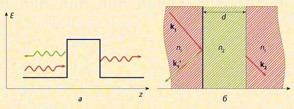
Rice. 5. Schematic representation of tunneling
electron through a potential barrier (a)
and a photon through a medium with a reduced refractive index (b).
This well-known optical effect is usually interpreted in terms of the quantum tunneling effect. It is said that a photon tunnels from one medium to another in the same way as an electron from one potential well to another. Here, as noted above, optically dense media serve as analogues of potential wells for photons, and an optically less dense medium serves as an analogue of the barrier between them (Fig. 5). The tunnel effect of photons is widely used in integrated optics to provide optical communication between different optical channels*.
* In fact, everything happened exactly the opposite. First, the "tunnel effect" in optics was discovered and studied. This achievement belongs to Academician L.I. Mandelstam. Much later (1927), he and his student, the future Academician M.A. Leontovich, extended the result obtained to electrons. The term "tunnel effect" appeared even later.Inside a photonic crystal
To clarify the qualitative side of the matter, just as it is done in physics solid body, consider a one-dimensional chain of optical microcavities with a distance between them equal to d and a distance between the centers of neighboring microcavities equal to a.
Let E 1 and E 2 be two discrete levels belonging to the family of allowed resonator levels. We also assume that the photons in the resonator can tunnel into the nearest adjacent (left and right) resonators. How will this affect the levels of E 1 and E 2 ? In solid state physics, the answer is well known: the discrete energy levels E 1 and E 2 turn into allowed bands, the width of which increases with increasing tunneling probability amplitude (Fig. 6).

Rice. 6. Formation of energy allowed bands from discrete levels w 1 and w 2 due to tunnel transitions.
If the photon energy is in the allowed zone, the photon propagates freely along the chain of microresonators, although the dispersion law relating the frequency and wavelength of the photon, generally speaking, is fundamentally different from that for a free photon. The appearance of a band gap is quite unusual for optics, the presence of which means that in a given frequency range, photons cannot freely propagate along the chain. The above reasoning naturally generalizes to two- and three-dimensional structures. It should only be noted that the distances between microresonators must be sufficiently small, and the refractive index of the medium filling the intercavity space must also be small so that photons of the forbidden frequency range cannot be found in it.

Rice. 7. Densities of photon states of a photonic crystal.
Area between w 1 max and w 2 min corresponds to the band gap, and w d - crystal defect
(see Fig. 10 below).
Figure 7 schematically shows the density of photon states g( w) for the considered model. The width of the zone is greater, the greater the ratio n 1 /n 2 . It is possible to choose the period of the structure and the values of n 1 and n 2 in such a way that the band gap is in the IR range, and in the visible region there would be a peak in the photon density of states. Such a photonic crystal would be an ideal material for a thermal light source. Particularly interesting in this regard is a metal photonic crystal - a periodic structure made of metal with high temperature melting (for example, tungsten), immersed in a transparent dielectric medium or air. A similar system was recently proposed independently by a group of Italian and Russian researchers from the FIAT research center and American scientists from the Sandia laboratory. According to calculations by American scientists, the use of a tungsten photonic crystal can increase the efficiency of an incandescent lamp from 5 to 60%. This would lead to huge savings in energy and lighting costs, and in addition would reduce the environmental burden due to useless heating. environment. In addition, by managing spontaneous emission atoms and molecules, it is possible to improve the parameters of optoelectronic sources and lasers. We also note an interesting experimental fact discovered by researchers from Sandia: a photonic crystal converts incident infrared radiation into visible light, which is very useful for increasing the efficiency of solar cells. Finally, a photonic crystal can be used as a broadband light filter (Fig. 8).
There is some subtlety in the concept of the bandgap of a photonic crystal - the central one in this discussion. As already mentioned, there are three types of photonic crystals - 1D, 2D and 3D crystals. The total bandgap for photons exists only in three-dimensional photonic crystals. The word “complete” means that the band gap is realized for arbitrary orientations of the wave vectors, i.e. for photons propagating in an arbitrary direction (Fig. 9a). In two-dimensional and one-dimensional photonic crystals, the band gap exists only for photons that propagate in a certain solid angle, which is rather wide in the former and much smaller in the latter (Fig. 9b). Despite the “inferior” nature of such zones, they are also of interest for applications, since they have many characteristic features complete band gap.
Rice. 9.Schematic representation of the processes of light propagation from a point source,
located in a photonic crystal with full (a) and partial (b) band gaps.
It is known that defects in crystals, such as vacancies, foreign atoms, and dislocations, can lead to the appearance of allowed levels in the band gap. Similar levels correspond to localized states of electrons. A similar situation is realized in photonic crystals. Vacancies can also act as defects; empty elements in the lattice, or elements filled with a material with a different refractive index. These types of defects are called point defects, but in fact they are microcavities or microcavities that can capture or localize photons and are of great interest for creating efficient point light sources, in particular lasers with a low generation threshold. There are also linear defects, which, for example, are filamentary cavities inside a photonic crystal. Unlike point defects, linear defects can conduct light along themselves (Fig. 10). In fact, they are optical waveguides: even if they are strongly bent, such defects will ideal conductors photons - they "lead" the light without loss! It is not surprising that they receive so much attention in optical communication technology.
Rice. ten. 2D photonic crystals. Light-guiding channels and optical fibers.
The analogy between the quantum behavior of electrons in semiconductors and photons in crystals has a rigorous mathematical justification: after simple transformations, Maxwell's equations can be represented in a form that is formally identical to the Schrödinger equation for the electron wave function. It was this analogy, which Yablonovich drew attention to, that became the source of many ideas in the development of the physics of photonic crystals. Moreover, it turned out that the processes in photonic crystals are amenable to computer calculations with a much higher degree of reliability than the corresponding problems for electrons in a crystal. This is due to one of the fundamental differences between photons and electrons - electrons have a much stronger interaction between themselves than photons. Therefore, “electronic” problems require taking into account many-electron effects, which greatly increase the dimension of the problem, which often forces the use of insufficiently controlled approximations, while in photonics this difficulty practically does not exist.
How photonic crystals are made
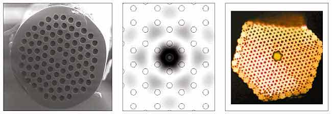
The production of photonic crystals for the visible wavelength range (Fig. 11) is very difficult problem, since the lattice constant of such a crystal should be comparable with the wavelength of light, i.e. lie in the submicron region. The submicron region is now being actively explored by microelectronics based on planar technology, but here we are talking about the creation of already three-dimensional periodic structures with a submicron period. Recall that this length is more than 100 times less than the diameter of a human hair. There are currently two ways to produce photonic crystals. The first, sometimes called “top-down” for short, is based on lithography, which is widely used in microelectronics for the production of semiconductor integrated circuits. This complex method, which requires very expensive equipment, but at the same time is very accurate and flexible, allows, in principle, to create arbitrary structures and is certainly promising. Impressive results have recently been achieved here. These include the aforementioned metal (tungsten) photonic crystals with a very wide total band gap in the range from 8 to 20 μm. The period of the 3D photonic crystal was 4.2 µm, the thickness of the elements was 1.2 µm. To create a photonic crystal with a band gap directly adjacent to visible range, it is necessary to go to the nanometer region.

Rice. eleven. Typical Structures of 3D Photonic Crystals.
Another “bottom-up” path, based on the spontaneous crystallization of a colloidal solution of small particles and called self-assembly, provides a fast and relatively simple method for manufacturing photonic crystals. The self-assembly method is mainly used to create dielectric photonic crystals. For example, at the first stage, a three-dimensional periodic structure is grown from a colloidal solution by self-assembly from polymer or quartz (SiO 2 ) microspheres, which is further used as a matrix for manufacturing a periodic optical medium with specified parameters. At the next stages, the voids of the matrix are filled with a material with a high refractive index, after which the microspheres are removed by chemical etching, which solves the problem.
The disadvantages of the method include a small variety of types of periodic structures (matrices) obtained. In addition, it is quite difficult to get rid of random defects that “spoil” the band gap, but it is not easy to create artificial structural defects that modify the band in the desired way. However, in recent years, Ya. Vlasov and his colleagues from IBM have proved that these obstacles can be overcome. They grew large (about 1 cm in size) and very perfect photonic crystals on the silicon surface, clearly demonstrating the presence of a band gap in them. Moreover, scientists have learned to form artificial defects in them. All this, as well as the fact that photonic crystals are grown on the surface of silicon, the main material of microelectronics, is very encouraging. Moreover, Nature has already worked in this direction.
Recently, physicists from St. Petersburg and Minsk have found interesting and deep analogies in the properties (behavior) of photonic crystals and a natural mineral - opal, which also consists of densely packed quartz spherical particles, although it does not have a regular periodic structure. Opals have long been known for their delightful play of colors, which, like in a photonic crystal, arises from the diffraction of light on the structure of quartz spheres.
Australian scientists from the University of Sydney have discovered that photonic crystals are found in the living world, namely in a sea worm that lives in relatively deep sea waters. The sea worm is covered with “fur” of needles with a bright iridescent color, which shimmers and plays depending on the angle of incidence of light and the angle of observation (Fig. 12, a, b, c).

Rice. 12. sea worm Genus aphrodite(a), its iridescent needles (b, c)
and a cross-sectional image of the needle in a scanning electron microscope (d).
Studies using a scanning electron microscope revealed the presence of a 2D periodic structure in the needles (Fig. 12d), probably with an incomplete band gap. Here, just as in opal, the play of color is determined by the diffraction of light on a complex microstructure, and not by the dispersion of the absorption and reflection coefficients on certain dyes.
Some butterflies (eg. morpho rhetenor, South America) iridescent coloration of the wings is also due to the diffraction of light on the microstructure of the scales of their wings (Fig. 13).

Rice. 13. Butterfly Morpho rhetenor and details of the selected section of its wing.
These discoveries inspired researchers from Marseille and Amsterdam to develop new types of fabrics, the color of which is created not only by certain pigments, but also by a specially designed microstructure; they also attract engineers from the automotive industry. optical effects, characteristic of 2D photonic crystals, can also be searched for in the reflection spectra of silk carpets made by skilled craftswomen from Kerouan (Tunisia). The density of knots in them is about 106 m–2, and their color shimmers brightly and bizarrely in the sun when the angle of incidence of light changes. Here, obviously, the matter is also not only in the pigment, but also in the diffraction of light.
But back to the problems of photonics. If we want to process information and transmit it using photons, just as electrons do for us, we need to learn how to control photons somehow. Although they do not have an electric charge, but the presence of polarization, i.e. orientation of their electromagnetic field, gives some hope of success.
The Path to Polarization Control
From a quantum mechanical point of view, the concept of polarization of light is associated with the presence of a spin in a photon. Photons, as particles with zero rest mass, can be in two states with values of the moment ±ћ, directed along the momentum of the photon; such photons have circular polarization: left (quantum number
m = +1) or right (m = –1). Elliptically polarized photons are in a state that consists of states with m = ±1; for linear polarization, the superposition of these states is such that the average projection of the momentum onto the momentum direction is zero.
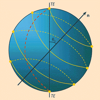
So, the photon is a two-level system, i.e. system described by the quasi-spin S q = 1/2, the direction of which in space is determined by the polar ( a) and azimuthal ( b) corners. In other words, the set of polarization states is uniquely mapped onto the set of directions given by the angles a and b, or, equivalently, to the set of points belonging to some sphere, which in optics is called the Poincaré sphere, and in quantum physics- Bloch sphere.
For a free photon, the states m = +1 and m = = –1 have the same energies (frequencies). In quantum mechanics, this situation is called degeneracy. The degeneracy can be removed using an external magnetic field directed along the wave vector (it is assumed that the photon propagates in a medium with a refractive index n): in the field, the components with m = ±1 will propagate with different velocities:
u ± = (c/n)(1 ± Q). (four)
As a result, circular birefringence (gyrotropy) of the medium takes place in a magnetic field. The magneto-optical parameter Q, proportional to the magnetic field in non-magnetic media, has a typical value of ~10 –6 -10 –4 . In magnetic materials, the parameter Q is nonzero even in the absence of a field and reaches values of 10–3 -10–1.
In this case, the well-known Faraday effect is observed experimentally; rotation of the plane of polarization of linearly polarized light as it propagates in a medium along a magnetic field. Its rotation angle (Faraday angle) is equal to
q F = ( w/c)nQL = 2 p LQ/ l, (5)
where L is the sample length, l= c/ w n is the wavelength of a photon in the medium. This is how a free photon behaves in a magnetic field.
The Faraday effect is one of the most effective methods photon properties control. It is already widely used in laser technology, computer science and other fields. How does it manifest itself in the case of trapped photons?
The behavior of a trapped photon in a magnetic field differs significantly from that described above. First of all, we note that the presence of a geometric framework limiting the motion of a photon, in itself, as a rule, removes the degeneracy of the states m = ±1 of the photon. Consider, for example, the propagation of a photon in a thin film consisting of a transparent material with a refractive index n. In this case, the states with m = ±1 split in such a way that there are
two differently polarized modes TE and TM, the propagation speeds of which are different - u TE and u TM . In the first mode, the electric field is directed perpendicular to the direction of photon motion, and in the second, the magnetic field. The electromagnetic field in such a waveguide can be represented as a superposition of two close TE and TM modes.
As for a free photon, a magnetic field (or the magnetization vector of a transparent magnetic material) directed along the waveguide causes transitions between modes. For example, if a TE mode enters the “input” of a transparent dielectric waveguide, then due to the gyrotropy induced by the magnetic field, it gradually (as it propagates) passes into the TM mode (but usually not completely), then back into the TE mode etc. This is how the Faraday effect is realized in a film waveguide. The conversion efficiency is naturally limited by the light absorption coefficient and the splitting of the TE and TM modes, i.e. the difference between u TE and uu TM . The larger the splitting value, the lower the mode conversion efficiency, i.e. the smaller the resulting value of the angle of rotation of the plane of polarization of light.
A similar mechanism of the Faraday effect - the conversion of TEЫ TM modes - is realized in two-dimensional photonic crystals. As with waveguides, in order to achieve the maximum magnitude of the Faraday effect (or the maximum efficiency of light control), it is necessary to match the TE and TM modes, i.e. bring their phase velocities closer together.
In photonic crystals, another interesting opportunity arises to enhance the Faraday effect. As we have shown, for this it is necessary to “work” at the boundary between the allowed and forbidden zones, where the propagating waves critically slow down, which leads to an increase in the corresponding effects due to an increase in the wave-crystal interaction time.
Quantum mechanical analogy
Attention is drawn to a very close analogy between the considered picture of the behavior of a photon in a waveguide and the two-level system of quantum mechanics. An important characteristic of a two-level system is the quasi-spin S q (or the Bloch vector). The dynamics of Sq is determined by a simple equation: ¶ S sq / ¶ t = , (6)
where A ef is the effective field acting on the quantum system. Equation (6) describes the motion of the vector S kv along the Bloch surface. The equation for the quasi-spin, which describes a photon in a waveguide or a periodic medium, looks like (6), but instead of time, you need to use the coordinate along the photon propagation path:
¶ S sq / ¶ x = , (7)
where F eff is the effective field acting on the photon spin. The difference is that quantum electronics uses fields that depend on
on time, and in photonics - on spatial coordinates. This quantum-mechanical "spin" analogy was noted and substantiated at about the same time as Yablonovich's analogy, which led to the creation of photonic crystals. It is logical to expect that quantum effects well known for two-level systems, such as nutation, p-pulse, Han echo and others, have spatial analogs for a photon propagating in specially created spatial structures such as photonic crystals. Is it really?
Equation (7) gives the key to achieving the maximum efficiency of mode conversion in magnetic waveguides, just as in quantum electronics, using the so-called p-pulse, a similar problem is solved - population inversion of a two-level system. Let us consider the harmonic modulation of a magnetic field that exists in a waveguide (in a magnetic material, such modulation can be created by exciting a standing magnetostatic wave in it). If the modulation wavelength a and the difference between the wave vectors of the TE and TM waves D k are consistent, so that aD k = 2 p, then the rotation of the Bloch vector over the sphere (Fig. 14) occurs practically along the meridian, and the degree of mode conversion (or the Faraday rotation angle) depends linearly on the wavelength of propagation of the wave. For a complete conversion, for example TE® TM, or vice versa, a length is sufficient at which the vector S kv reorients from the north pole to the south, or vice versa, i.e. at a reorientation angle S kv equal to p. In practice, waveguides with alternating direction of magnetization are usually used (Fig. 15), which can be chosen in such a way as to achieve a reorientation of Sq between the north and south poles spheres (Fig. 14), i.e. with 100% conversion mod.
Rice. fourteen. Image on the Poincaré sphere of the mode conversion process in waveguides with alternating change in the direction of magnetization. The dotted line shows the trajectory of the Bloch vector for the harmonic distribution of magnetization.There is also an analogue of the spin echo. American physicist E. Khan, who owns the honor of discovering this phenomenon, offered its figurative explanation. Let a line of runners start at the stadium at time t = 0, and then everyone runs with their own, but constant, speed. After some time, due to the difference in speeds, the line crumbles along the treadmill. If at the time t give a signal that the runners turn around and run back, then at time 2t they will again form a line at the start. The role of runners in spin resonance is played by the spin moments of particles that precess (“run”) around the magnetic field with somewhat different frequencies. Spin echo is widely used in quantum electronics.
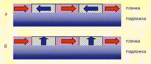
Rice. fifteen. Magneto-optical waveguides with alternating change in the direction of magnetization in the waveguide film along the x axis (a) and along the x and z axes (b); the arrows show the directions of magnetization.A similar experiment can be done with photons. Let us consider the scheme of the experiment shown in Fig. 16a. Elements U and V are two identical birefringent crystals of equal thickness. Let a polychromatic light beam fall at the entrance to the medium U, linearly polarized at an angle of 45° to the x and y axes of the crystal. At the exit from the crystal U, each spectral component of the beam will in the general case have an elliptical polarization. The entire light beam as a whole will be depolarized due to dispersion. This state of polarization is analogous to the complete loss of the macroscopic magnetic moment before the impact of the second pulse in the Hahn echo phenomenon. If the axes of the crystal V are rotated by 90° relative to the axes of the crystal U, then the result of the propagation of light in the second crystal will be the complete restoration of the state of light polarization at the exit from the crystal V, i.e. the polychromatic beam will again be linearly polarized.

Rice. 16. Geometry of the experiment on the observation of a spatial photon echo; general scheme (a), when using an electro-optical crystal (b) and on anisotropic optical waveguides (c) .Electro-optical crystals can also be used to observe the effect. The role of elements U and V can then be played by separate sections of the same crystal, if an electric field is applied to them in mutually perpendicular directions (Fig. 16b). A similar effect is also possible in anisotropic optical waveguides, in which the TE and TM modes are coupled (Fig. 16c). In the case of optical waveguides, the effect will be pronounced due to the strong dispersion, and the experiment can be carried out in a narrow spectral range.
* * *
I would like to end the article with a well-known historical anecdote. The Queen of England, having become acquainted with Faraday's discoveries in the field of electromagnetism, asked him about their practical use. To this Faraday replied: “Your Majesty, what can we say about the future achievements of the newborn?”
11. Zvezdin A.K. Brief communications on physics FIAN. 2002. V.12. pp.37-50.
12. Klyshko D.N. Physical foundations of quantum electronics. M., 1986.
13. Zvezdin A.K., Kotov V.A. Magneto-optics of thin films. M., 1988; Zvezdin A.K., Kotov V.A. Modern magnetooptics and magnetooptical materials // IOP Publishing. 1997. Bristol and Philadelphia.
14. Akhmediev N.N., Zvezdin A.K.// Optics and spectroscopy. 1989. V.65. pp.487-489.


